When manufacturing printed circuit boards (PCBs), various issues can arise, but most are preventable or correctable. It is crucial to pay attention to these issues and take measures to avoid problems down the line. One of the most significant challenges in PCB assembly is warpage, which, if left unattended, can lead to stretched joints and unfit boards.
Understanding Warpage
PCBs are designed to be flat, providing a stable surface for mounting components and connecting traces to create functional circuits. Whether single or multi-layered, the flatness of the board is a fundamental requirement. Warpage in a PCB occurs when it becomes twisted, bent, or warped, causing it to deviate from its flat form. Warpage can manifest as either a bow or a twist.
- Bow: In the case of bowing, the board forms a single arch, either upward (positive bow) or downward (negative bow), along one axis.
- Twist: A twist warpage causes the board to bend in both the lengthwise and widthwise directions, creating a combination of positive and negative curves. This curvature disrupts the alignment of traces, components, and holes on the board’s surface, leading to numerous assembly problems.Warpage primarily affects the assembly process, resulting in incorrect component placement, stretched or open joints, solder bridges, solder flooding, and incompatibility with the final build due to dimensional deviations. This issue hampers the proper functioning of automated placement machines and soldering processes, potentially leading to short circuits and improper connections.
Causes of Warpage
Warpage in PCB production typically arises from two main factors: excessive physical stress and coefficient thermal expansion (CTE).
Excessive physical stress can result from improper stacking or securing of the board. For instance, if a board is stored incorrectly, placed under excessive pressure during storage, or clamped too tightly in a frame during assembly, it may become permanently bent.
CTE-related warpage occurs due to differences in the expansion rates of the board’s copper traces and the substrate material. When subjected to temperature changes, these disparities in expansion rates lead to the board warping.
Regardless of the cause, once the warpage begins, it tends to worsen during the reflow/solder stage due to increased heating. However, you can predict and mitigate potential warpage issues with proper planning.
Preventing Warpage
While there are no industry-specific specifications for PCB warpage, general standards, like IPC-A-610E, specify that the maximum allowable bow or twist should not exceed 0.75% from the board’s original axis, resulting in a failed PCB.
To prevent warpage, PCB designers can consider the following factors:
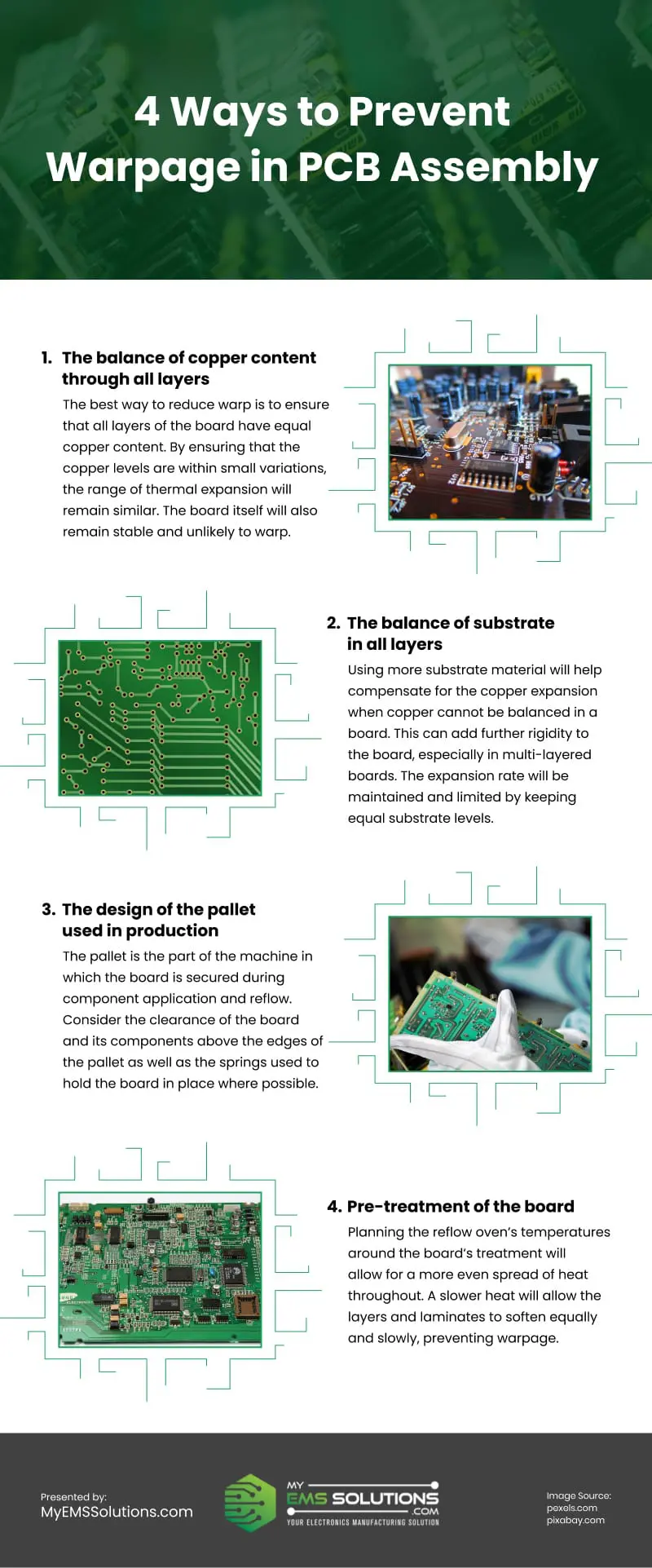
Balance of copper content: Ensure that all layers of the PCB contain a balanced copper content to maintain consistent thermal expansion.
- Balance of substrate: Keep the substrate levels uniform across all layers, or use additional substrate material to compensate for uneven copper expansion.
- Pallet design: Design the pallet used in production to avoid putting excess pressure on the board’s edges and consider clearance for components.
- Pre-treatment: Plan the reflow oven’s temperature profile to promote even heat distribution and prevent warpage during the soldering process.Warpage is a significant concern during PCB assembly, but it can be prevented with careful consideration and pre-planning. By addressing these key factors, PCB manufacturers can maintain the flatness of their boards and ensure successful assembly.source: https://www.myemssolutions.com/how-to-prevent-warpage-in-pcb-assembly/
Comments
Download this infographic.
