PCB manufacturing and design pose various challenges, with signal integrity preservation being a critical issue. When signals travel on a PCB, they often face distortion from factors like noise, which can be detrimental. Fortunately, a powerful solution to combat these issues is the use of back drill PCBs.
What is Back Drilling?
Back drilling is a technique used to maintain signal integrity in high-speed PCBs. It addresses challenges by carefully managing the architecture and production processes. One particular concern is transverse components, which are non-functional and can affect signal integrity by causing reflections. To overcome this, Depth Control routing PCB techniques are employed, involving re-drilling the PCB to remove stubs.
The Concept of Back Drilling
The concept of back drilling involves creating openings slightly larger than plated through-holes (PTH) to remove conductive material from stubs. It’s crucial to control the depth of the drilled holes to prevent signal reflections. Back drilling is also known as control depth drilling, as it regulates the depth of holes drilled.
Benefits of Back Drilling
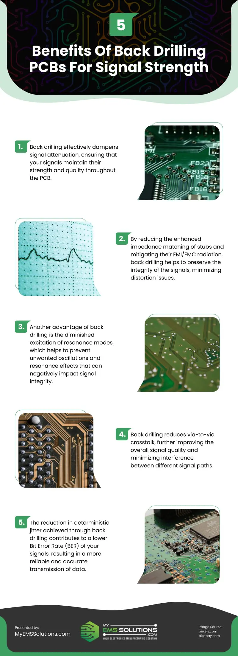
Using back drilling on PCBs offers several benefits. It helps maintain signal strength, reduces impedance matching issues and electromagnetic interference, prevents resonance effects, minimizes crosstalk, and lowers deterministic jitter for more reliable data transmission.
Limitations of Back Drilling
However, back drilling has limitations. Depth control is critical, as inaccuracies can lead to problems. External factors like drill-tip angle and board warpage also affect back-drilling depth. Attention to drilling methods and materials during production is necessary for accuracy.
Example of Back Drilling
Imagine a scenario where we have a 12-layer stack-up PCB with signals traveling from layer 1 to layer 12. However, we only want signals to go from layer 1 to layer 3. Unfortunately, after layer 3, there’s extra material leading to unwanted high-frequency repetitions and reflections, weakening the signal.
To fix this, the PCB manufacturer uses back drilling to remove the extra material between layer 3 and layer 12, making the signal path cleaner. The diameter of the back drill should be a bit wider than the gap to ensure all excess material is removed.
Here’s a helpful tip: Make sure the back drill’s width is slightly larger than the main drilling diameter. Usually, the back pin is 8 mils larger than the primary pin, with a length of 10 mils. Keep track and plane clearances high to avoid accidentally drilling into adjacent areas. It’s recommended to maintain a minimum clearance of 10 miles for planes and traces.
Setting Up Back Drilling
Setting up back drilling involves selecting specific sections for drilling, accessing the design menu, configuring settings, and adding or removing back drills as needed.
Effective Alternatives to Back Drilling
While back drilling is effective, alternatives like buried and blind vias or laser-drilled vias can manage stub length differently. Proper setup and attention to detail ensure successful implementation of back drilling, ultimately enhancing signal integrity in high-speed PCB designs.
In conclusion, back drilling is a valuable technique for PCB manufacturers to ensure signal integrity in high-speed designs. By carefully controlling stubs and reflections, back drilling optimizes PCB performance, meeting the demands for reliable data transmission in modern electronics.
source: https://www.myemssolutions.com/how-back-drilling-pcbs-can-improve-signal-strength/


